Precise and efficient
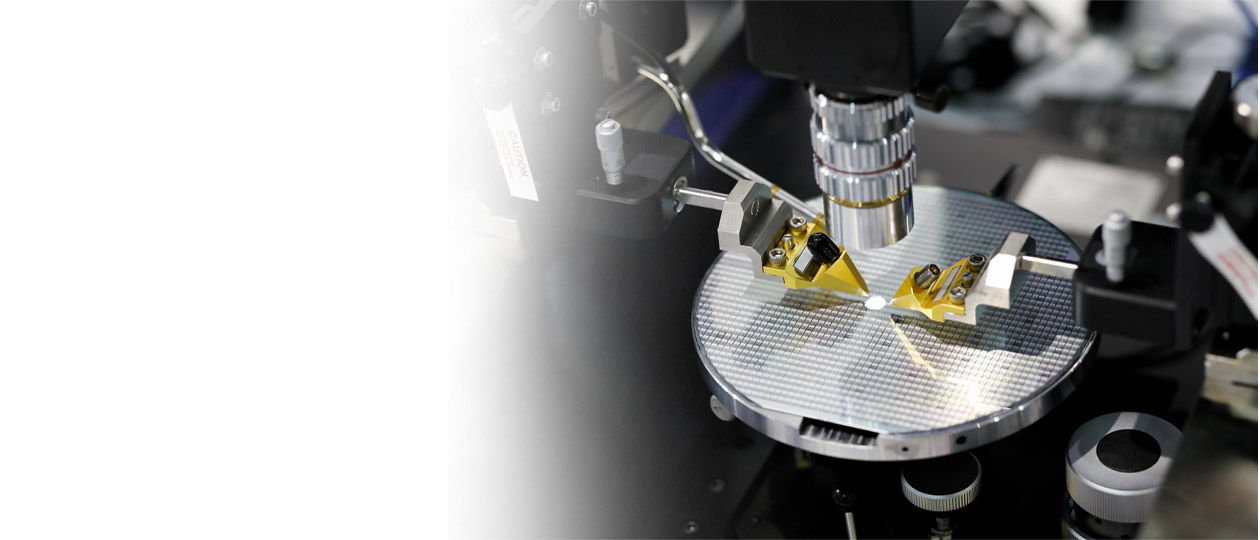
When inspecting optics at wafer level, in addition to precision, efficiency is of utmost importance, as a large number of optics must be checked and documented within the shortest possible period of time. Consequently, for reasons of economy, the inspection of wafer-level optics must therefore be automated.
Wavefront measurement technology is applied, for example, to check the image quality of individual lenses that are later used in smartphone lenses. Their tools and master molds are also inspected, e.g. by measuring the 3D surface shape through incident light.
Another example can be found in the inspection of microlenses with diameters down to 50 µm, where both image quality and surface shape as well as apex radius and conic constant can be measured using the corresponding testing configuration.
Fast and highly-automated
The wavefront measurement is based on a single camera image and is therefore very fast, and offers high intrinsic stability. Optocrafts measurement modules are a powerful, fully automated measurement solution for high volume production. The flexible communication interfaces supplied with the Shack-Hartmann software SHSWorks allow for a simple and fast integration into production lines, both mechanically and in terms of software.
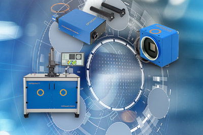
Our solution for the inspection of wafer-level optics
Systems and modules of the SHSInspect family measure the transmitted or reflected wavefront, thereby providing information on the imaging quality and focal length or on the surface shape and apex radius + conic constant of the lenses under test. Due to the single frame based wavefront reconstruction, the approach offers a very high intrinsic stability and is ideally suited for automation. SHSLab wavefront sensors deliver fast and precise measurements at a wide range of wavelengths.
additional Information